Projets:Lab:2015:SolderStation:ManuelEnglish
Contents
Assembly Manual
   Two files and six other Wiki pages are associated with this guide:

 *  les instructions de chargement du firmware (version Française
 *  Une presentation générale de l'appareil (version Française
 *  Le guide de montage illustré (version Française
 * File:BOM Station CMS.xls La liste d'achat au format xls
 * File:BOM Montage.xls La liste de montage au format xls

 *  Loading the firmware, English version
 *  Assembly Manual, English version
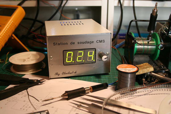
 *  A quick general presentation of the solder station(English version
The tools you need
- Soldering iron (with a fine “needle” tip)
- Solder wick (to correct bad solder points)
- Cutting pliers (“flush” cutting, not bevelled if possible)
- Solder flux
- Isopropyl Alcohol (small bottle)
- Toothbrush or Q-tip
- Jewelery tweezers or fine tip tweezers
- Solder wire (0.5mm max dia recommended, 0.3mm is better, tin-lead-silver or tin-lead-copper alloy. Try to avoid ROHS solder)
- Components (see BoM of the “kit number 2”)
- 2.5 meter cable wire
- Arduino Nano (NOT mini!)
- Power supply 12 V (for testing)
- Protection goggles
The first part of this manual deals with the assembly of SMD and through-hole components to build the heart of the solder station. It does not address the mechanics (boxed layout, integration) of this equipment.
      Important note: each step requires you to remove one or many (up to 9) component out of the
      kit. To avoid losing them, it is recommanded to put these devices in a small container (yogurt
      cup, plate etc).
      DO NOT extract the components from their storage tape more than one after the other
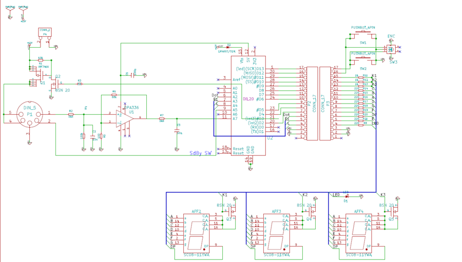
Schematic diagram and PCB ayout
Click on the picture to get a high definition version
The schematic is not very complex.
The heart of the device is an Arduino (Nano in this case). Ports D2 to D13 and A2 to A4 are devoted to man to machine interface, which can be completely modified depending of the user’s choice. Some people in the Electrolab have prefered to use a color LCD rather than the basic set of 7-segment displays. The choice of temperature controls (buttons "up-down" or rotary encoder) depends on a simple selection in the configuration file (see the “firmware installation” chapter). Both possibilities (button or encoder) have been kept on the pcb
The soldering iron plugs into P1. On this connector, you will find a 12 V “power” output (pins 4 and 5) supplying heating resistor of the iron. This voltage is not a DC voltage but a PWM signal controlled by the Arduino (D3 port) via a power FET transistor Q1. The duty cycle decreases or increases the proportion of current sent to the iron, and hence its temperature.
Also on P1, pin 1, a very low and variable voltage is received from the temperature sensor hidden in the body of the Weller solder tip. This voltage is strongly amplified by the operational amplifier OPA336, and then injected on one of the analog inputs of the Arduino. The value of this voltage gives a clear indication of the iron temperature to the microcontroller. The microcontroller then decides to increase or decrease the width of the PWM signal (port D3). This variations has for consequence the increase or decrease of the iron’s temperature as already mentioned.
The A5 port of the Arduino, named "STDBY SW" (standby switch) puts the iron in a "cold" standby position when this pin is grounded. Its activation may depend on of a magnetic switch (reed contact) hidden in the handle or the support of the soldering iron (the state of this switch is triggered by a magnet hidden in the support or the handle).
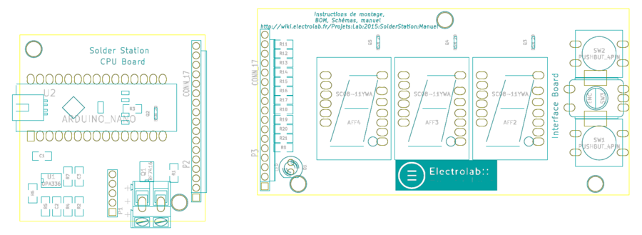
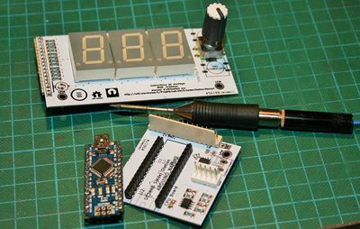
The entire station stands on two separate circuit boards. On the left of the schematic, the microcontroller card which supports both the Arduino Nano and components of the measuring loop (measuring amplifier, power supply transistor of the resistance of iron). On the left, a large 5x10cm PCB the man-machine interface (buttons/ temperature control encoder, digital display). This displays as two functions: it shows the iron’s temperature and the PWM duty cycle (decimal points: the more “dot point” you have, the wider the pwm is). An LED, located in the left lower corner of the display, will also light on when the iron is "heating".
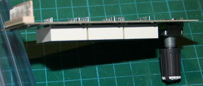
The flat “shoulder” of the encoder is at the very same level as the 7 seg. display. This way, the displays and the “Temp” encoder will flush with the the front panel of the station.
Use this layout diagram to identify the location of components during the assembly
The display board
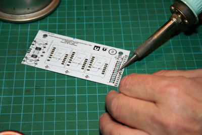
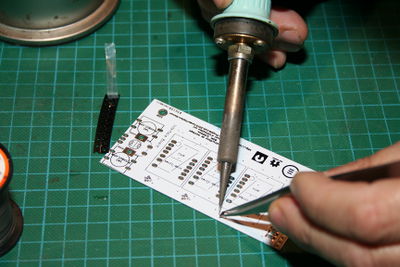
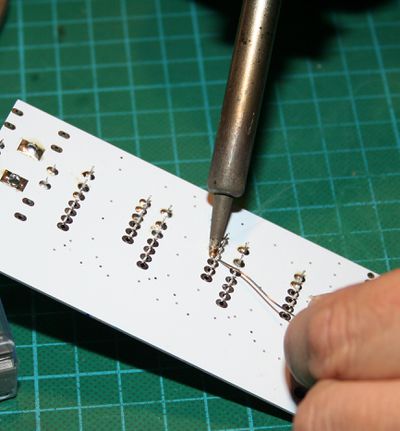
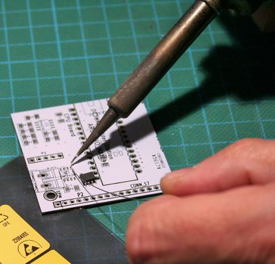
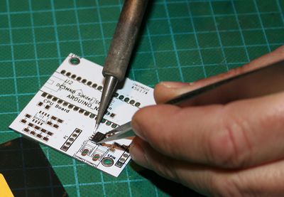
Put three small blobs of solder on the three upper left footprints R11, R12 and R13 of the display card (one side only, NOT the two solderpads). Use the tweezers to take 3x 1 kOhm resistors, gently slide each resistor in position while heating the solder blob with your soldering iron. Do not try to heath the component itself, just the pad. The metal will flow and “wet” the resistors. If the solderpoint is not shiny anymore or refuse to spread (by capillarity) on the resistor’s side, just add some solder flux. Once the metallized part of the resistance is "wet" by the solder, remove the iron while maintaining the tweezer ... without moving. That’s fine, you’ve made your first SMT solder point.
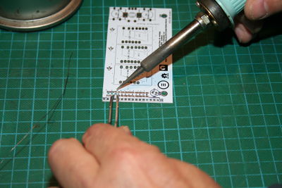
It is not advisable to leave the iron tip in contact with the printed circuit during a long period of time (5 seconds maximum).
Solder drop must spread on the end of the component by capillary. If this is not the case, either the soldering iron is not enough clean (wipe it with a sponge or bronze wool) or the solder itself is oxidized (in this case, add a drop of flux).
Repeat the operation for the second 1 kOhm resistors… and so on. The three resistors once maintained by the solder on the board, solder the other side of each resistor.
At the end of this operation, you still have one 1k resistor left in its protective tape. Take it preciously apart. You’ll need it when building the MCU board.
Take 9x 220 Ohm resistors (R14 to R21 and R8), and repeat the operation for the next 9 resitor’s locations.
Beware not to "overload" the solder pads. Too much solder could provoke bad electrical contacts
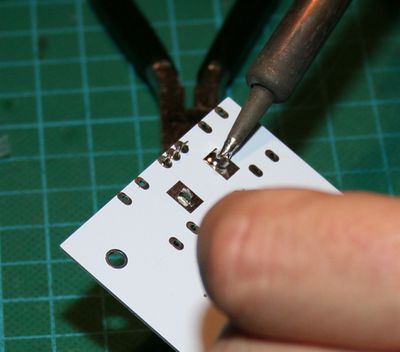
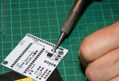
Take 3 x BSN20 FETs (Q3, Q4, Q5). Put a drop of solder to only one of the three pads (the one located in the middle is the most convenient). Then hold the transistor by the sides with your tweezers and slide it into the drop of molten solder (well… not the component itself, just the pin ;- ) ). Take off the board the tip of your soldering iron when your transistor is in the right position. All the three pads must be aligned with the corresponding pins of the device. Wait two or three seconds until the solder is cold and solid. Make sure the transistor is centered and all it’s pin on a solder pad. If this is not the case, correct its position again by heating the solder bump and try to adjust the position of the transistor again. . Repeat this for all three transistors located on the upper edge of the plate
DO NOT over tighten the tweezers. By clenching too much, you may see your component literally “catapult” out of your tweezers, due to the elasticity of steel.Thus catapulted, the component status changes and turns into “meat for vacuum cleaner” ... you’ll have to take another transistor because the chances of retrieving it are inversely proportional to the importance of the said component.
At the end of this operation, you have one BSN20 transistor left on its protective strip. Take it apart too, with the 1k resistor (see first chapter above)
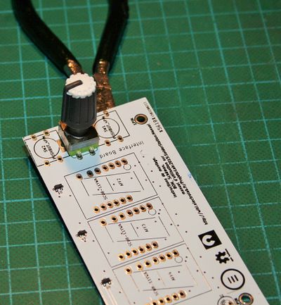
Put the SW3 rotary encoder in it’s place, on the right side of the pcb. The case must firmly rest on the surface of the pcb. If not, the upper surface of the display won’t flush with the surface of the front plate of your enclosure.
Soldering this component should not be a problem. Except perhaps a lowering of the temperature of the tip of your iron when attempting to solder the two metallic side tabs. If you have a second soldering iron, use a larger solder tip and a thicker solder wire of 0.5 mm
Position the three 7 segments displays AFF2, AFF3, and AFF4. They can only be installed in one only one position/orientation. Be careful not to bend one of the pin when inserting each display unit.
Solder each pins after returning the board. Take care that the base of the component remains in contact with the pcb. Again, a large iron tip and a solder wire of 0.5 or 1mm is appreciable
Install
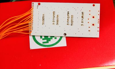
- either a Molex kk 15 contacts connector (optional) on the opposite side of the components and board (see picture)
- Or 15 pieces of wire, 15 cm each (approx. 6 inches). Strip each end over 4mm, tin with a solder drop, and insert and solder these wires one by one in the holes provided for this purpose.
Trim each wire with a cutter plier.
Warning: the last two holes located on the bottom of the row must stay free of any wire. They are reserved for possible extensions between the interface and a gpio Arduino (one GND and one "free" wire).
Picture above : the wiring once finished (click on the picture if you want a higher resolution)
Using "kk" Molex connectors (optional) may seem attractive. In fact, it’s just a bad idea: the wiring of the cable itself with it’s two “housing” is long and tedious (especially for those not accustomed to this kind of sport) and insertion force needed to connect the whole 15 pins connectors is really high.
Solder the Led D1 located at the left hand side of the pcb. The longer wire goes on the upper hole, the shorter in the lower (grounded) hole. The top of the LED should slightly protruding above the level of the 7 segment display.
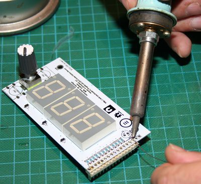
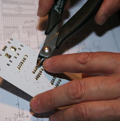
With cutting pliers, cut/trim protruding pin and wires
Always keep a finger on top of the pin being cut (see photo). Metal shrapnel could be thrown when cutting the pin causing potential serious injuries. Protective eyewear is strongly recommended
This conclude the assembly of the first pcb
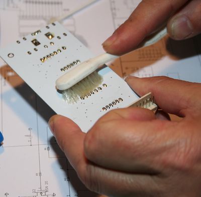
Clean flux residues with a toothbrush or Q-tip soaked in isopropyl alcohol (isopropanol or rubbing alcohol). Put the diplay board apart.
Cleaning is not just to have "beautiful" circuits. The solder flux is relatively acidic and over time could attack the copper tracks and contacts, causing outages and poor contacts.
MCU board
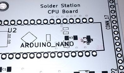
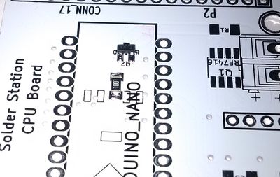
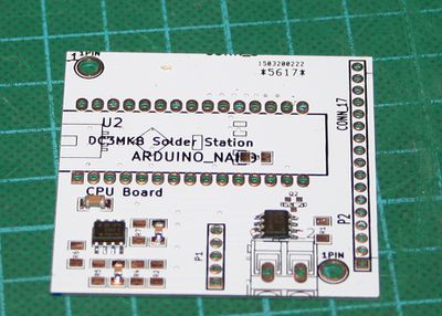
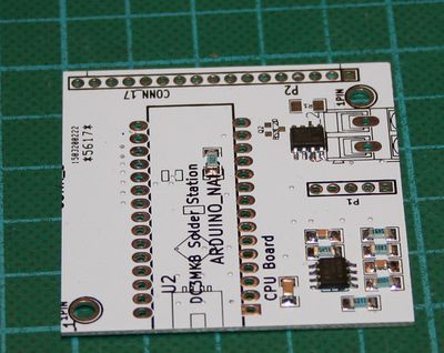
Remembrer, when assembling the display board. Two component have been take apart: a 1k resistor (R3) and a BSN20 transistor (Q2). It is wise to solder them immediately to avoid losing them, particularly if they have been removed from their protective tape.
Place the remaining transistor in the same way that you have already soldered the other (location of Q2 is between the two rows of HE10 female contacts of the Arduino Nano board)
Then the 1kOhm resistor
Now it's time to get serious and solder the first SOIC component
Active components in SOIC packages have an orientation. The number 1 pin is marked by a small laser etched “dot”, and/or a biased edge to 45 ° (see above picture)
Take the "MCU" board, the Q1 transistor (FET IRF7416). Important Warning : the kit includes two circuits with the same kind of packaging. Check the reference before soldering.
Proceed exactly as for the transistors by depositing a drop of solder on one pad only.
slide the component in position using the tweezers; while heating the solder drop with your soldering iron.
When the component is correctly aligned (all pins and pads) remove the tip of the iron so that the solder solidifies. Attention, an 8-pin SOIC case is a little bit more difficult to align than a transistor. The 8 component’s pins must be centered on each solder pad. One the first pin is soldered, take the opportunity to check again the orientation of the IC ... spotting the beveled side of the circuit is not obvious.
If everything is ok, solder the diametrically opposite pin of the component. Check centering legs and pads, adjust slightly if necessary. Then solder the other remaining six pins
It is common for beginners to create "bridges" between IC’s pins, bringing too much solder metal. Do not try to immediately eliminate the short circuit. Finish all the soldering of the other pins. Once this work is completed, put a drop flux over the bridge (a bridge is always a sign of poor "wettability" of the eutectic), carefully clean the tip of your iron and melt the solder overflow with the tip of the iron and some solder wick. The bridge will be literally sucked by the wick. Put some new and fresh solder if the braid has done his job too well. Go to the next solder bridge if there is one.
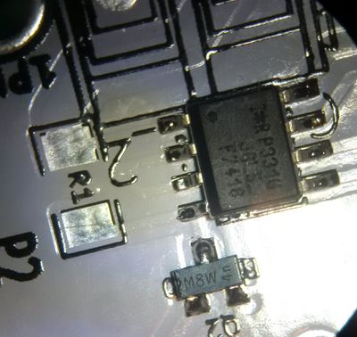
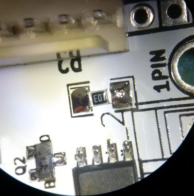
The next picture shows the IRF7416 soldered Do not pay attention of the transistor located close to Q1. This is Q2, BSN20, in prototype version of the pcb. Q2 is now placed between between the two pinout rows of the Arduino and has already been soldered (see beginning of this chapter).
Take the second integrated circuit U1 (OPA336), check its orientation (use orientation’s marks on the silk mask), then solder it as explained before.
Solder the 3 ceramic capacitors the same way you did with the resistors. Begin with the 100nF C1, then the two 10nF C2 and C3. Attention ! unlike resistors whose value is printed on the body of the component, capacitors are not "marked". Do not mix the values during assembly.
Do the same with the resistors R2 and R7 (5.6 kOhm), R4 (100 kOhm), R5 (100 Ohm), R6 (68 kOhm) located around the OPA336 operational amplifier. Then solder R1 (10 kOhm, near the IRF7416). R3 resistance (1 kOhm) close to Q2, under the Arduino Nano, has already been soldered.
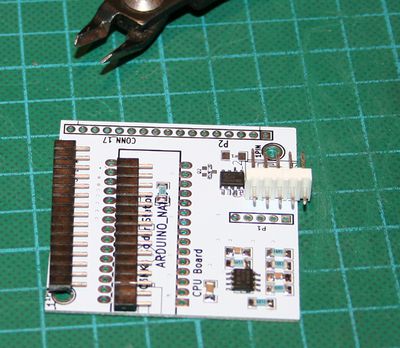
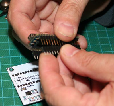
Prepare the two “15 contacts” Arduino support (female HE10)
Insert each row on Arduino’s pins. Make sure the connectors are fully inserted.
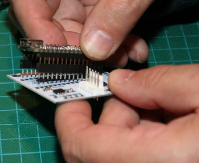
Insert the two strips maintained by the Arduino on the pcb.
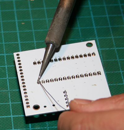
Solder the first pad, make sure the contact strip is resting on the “components side” of the pcb. Solder the pin located in the opposite corner.Make a final visual check, adjust if necessary, then solder all the pins.
This method guarantees a perfect alignment of pins. Do not try to solder the 15 pin connector without an Arduino that could be used as a “jig”
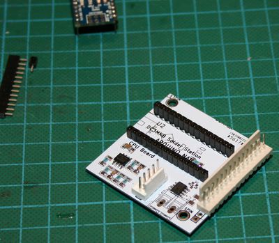
Optionally, it is possible to add two KK Molex connectors one of 15 (or 17) pins to connect the display unite, the other one with 5 pins to plug the output/soldering tip/temp. sensor connector.
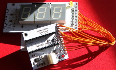
By default, these two connectors are NOT provided in the kit. It is easier to connect the Microcontroller, output connector and the display unit with simple cabling wires. (see picture above)
As for the display board, the two bottom holes are not used and therefore are not wired.
No wires should be crossed, the wiring is "straight, pin to pin." An exception: the two wires located at the top of the row (gpio 12 and 13). This two wire can be twisted so that the temperature increase is done by turning the encoder’s button clockwise. (with a “straight” cabling, increase of the temperature is set counterclockwise).
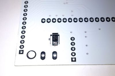
Flip the MCU board upside down and solder D2, a large CMS Schottky diode, taking care of the orientation. The cathode –marked with a bar on one end of the component- is oriented toward the Arduino side. The anode, the other side, is facing the 12 V pad and the pcb edge (in case of doubt, refer to the picture).
The electronic part is completed. It remains to be tested, after connecting the iron (see diagram) and loading the Arduino with it’s code (see the section “Programming Manual”). Once tests are successful, put the project in a box.
Loading the firmware
see the dedicated chapter
